
Programme Overview
Unlock the potential of digital VLSI design with our advanced certification course. Dive deep into RTL design, synthesis, and testing while gaining hands-on experience with industry-standard tools. Led by experts from IIT Delhi's Centre for Applied Research in Electronics, this programme equips you with the skills to excel in the blooming semiconductor industry.

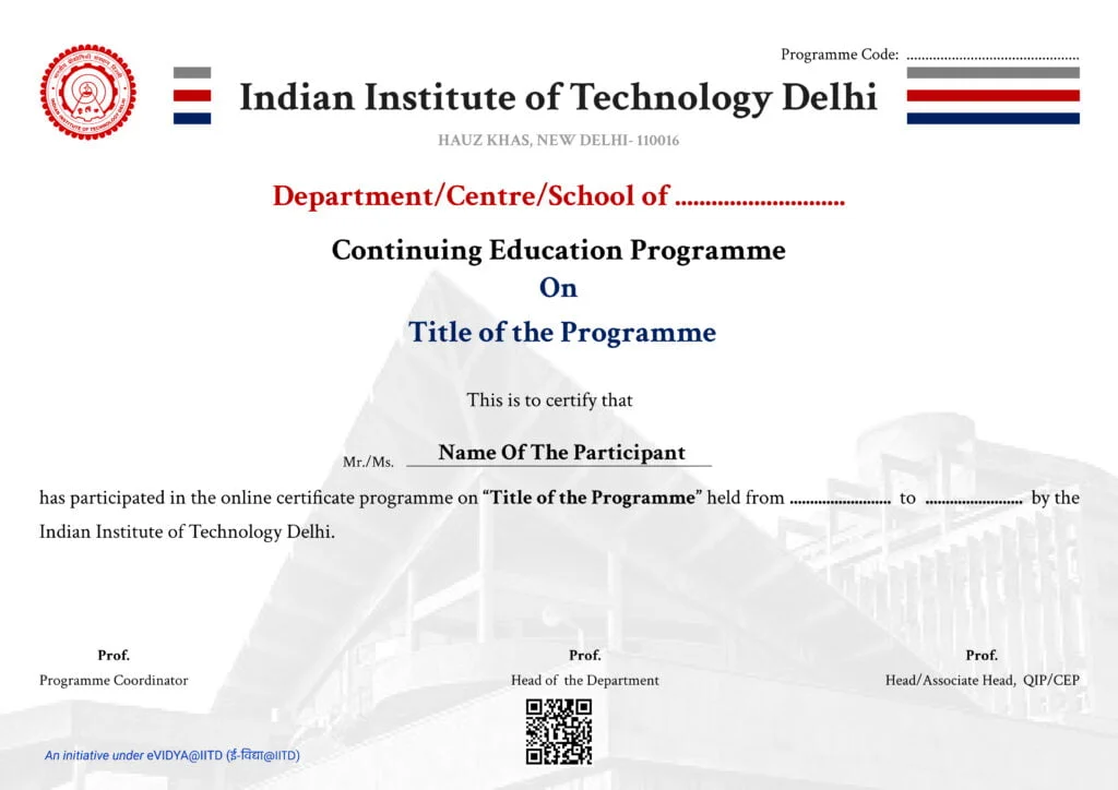
Certification from CEP, IIT Delhi

Learn from top faculty in VLSI Design

3 Days Campus Immersion

Real-world Case Studies

Industries Visits/Interactions with the Leaders
Networking Opportunities during Campus Immersion


.png)
Programme Content
MODULE 1: Digital IC Design
Module 2: Digital Circuit and RTL Design
Module 3: Physical Design
Module 4: AI/ML Hardware Accelerations
Module 5: Industry Specific Applications
Module 6: Scripting for VLSI Professionals
Lab Module
Tools
Projects
Some of the projects planned are given below:
Note: This is an indicative list of course topics and is subject to change as per IIT Delhi’s discretion.
Admission Fee & Financing
Easy EMI Options Available
Pay in easy monthly installments with our EMI options. No more worrying about finances; start your learning journey today!


Complete Payment
Participants can make one-time payment easily using options such as:


Eligibility
- Any Electronics, Electrical, Physics or Computer Science Graduate.
- Candidates pursuing the graduation degree are also eligible however preference will be given to applicants with experience.
- Diploma holders (10 + 3) or (10 + 2 + 3) are also eligible.
- Screening and selection will be done by IIT Delhi.
- 60% - End of programme MCQ-based exam
- 40% - Assignments & project
- 10% - Attendance (Grace)
- Candidates need to secure a minimum of 50% overall to be eligible for the certificate.
- Minimum of 50% attendance is mandatory.
Our Facilitators

Prof. Samaresh Das (Coordinator)
Professor & Head,
Centre for Applied Research in Electronics

Prof. Ankur Gupta
Associate Professor,
Centre for Applied Research in Electronics

Prof. Rahul Mishra
Associate Professor,
Centre for Applied Research in Electronics

Prof. Pushparaj Singh
Associate Professor,
Centre for Applied Research in Electronics
Programme Certification
- Candidates who score at least 50% marks overall and have a minimum attendance of 50% will receive a ‘Certificate of Completion’ from CEP, IIT Delhi.
- Participants who are unable to score 50% marks in the evaluation but maintain a minimum attendance of 50% will be eligible for the ‘Participation Certificate’ from CEP, IIT Delhi.
- The above e-certificate is for illustrative purposes only and the format of the certificate may be changed at the discretion of IIT Delhi.
- Only e-certificate will be provided and it will be issued by CEP, IIT Delhi.
- The organizing department of this programme is the Centre for Applied Research in Electronics (CARE) at IIT Delhi.

Certificate Programme in Digital VLSI Design
Programme by CEP, IIT Delhi
Gain practical experience with CAD tools and HDLs, preparing you for lucrative opportunities in semiconductor companies. Don't miss out – register today and take the next step in your career. Secure your future in digital VLSI now!
Apply Now